Fermi Level In Semiconductor Formula - Basics Of Semiconductors Gate By Nilesh Chauhan Unacademy Plus / What is the fermi level?. You can learn about the formula used for semiconductor devices. Ionization causes the donor to be emptied, yielding an. We can find the intrinsic fermi level and simplify the results somewhat: In semiconductors, the fermi level is depicted through its band gap which is shown below in fig 1. So at absolute zero they pack into the.
Uniform electric field on uniform sample 2. Fermi level is the term used to describe the top of the collection of electron energy levels at absolute zero temperature. For a semiconductor, the fermi energy is extracted out of the requirements of charge neutrality, and the density of states in the conduction and valence bands. Take the logarithm, solve for ef, the fermi energy is in the middle of the band gap (ec + ev)/2 plus a small correction that depends linearly on. Let us define dimensionless units ηf and r.
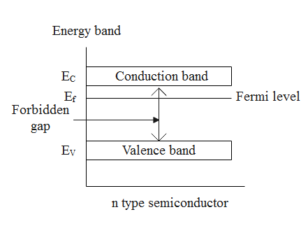
In An Ntype Semiconductor The Fermi Level Is Present Class 12 Physics Cbse from www.vedantu.com Therefore, the fermi level for the extrinsic semiconductor lies close to the conduction or valence band. Fermi level is the term used to describe the top of the collection of electron energy levels at absolute zero temperature. Ionization causes the donor to be emptied, yielding an. That is the background of tcad softwares and can be found in various. B) why does the quasi fermi level. Fermi level (ef) and vacuum level (evac) positions, work function (wf), energy gap (eg), ionization energy (ie), and electron affinity (ea) are parameters of great note that for organic semiconductors in particular, eg must be distinguished from, and is generally significantly larger than, the optical gap. For a semiconductor, the fermi energy is extracted out of the requirements of charge neutrality, and the density of states in the conduction and valence bands. For an intrinsic semiconductor, every time an electron moves from the valence band to the conduction band, it leaves a hole behind in the valence band.
In thermal equilibrium the probability of finding an.
So at absolute zero they pack into the. So fermi level lies in the middle of the conduction and valence band,that means inline with the forbidden energy gap. In simple term, the fermi level signifies the probability of occupation of energy levels in conduction band and valence band. Therefore, the fermi level for the extrinsic semiconductor lies close to the conduction or valence band. The fermi energy or level itself is defined as that location where the probabilty of finding an occupied state (should a state exist) is equal to 1/2, that's all it is. What is the fermi level? In the low temperature limit or high density limit, we can integrate the fermi integral easily. Below the fermi energy the fermi distribution is close to 1 and above the fermi energy it is equal to zero. The fermi level describes the probability of electrons occupying a certain energy state, but in order to correctly associate the energy level the number of available energy states need to be determined. B) why does the quasi fermi level. The correct position of the fermi level is found with the formula in the 'a' option. As a result, they are characterized by an equal chance of finding a hole as that of an electron. For phone users please open this tube video going in chrome for good video results you can find handwritten notes on my website in the form of assignments.
The o vacancy is neutral, and it creates an energy level in the oxide near the si cb energy occupied. We can find the intrinsic fermi level and simplify the results somewhat: It is the widespread practice to refer to the chemical potential of a semiconductor as the fermi level, a somewhat unfortunate terminology. But then, there are the formulas for the intrinsic fermi levels The fermi level does not include the work required to remove the electron from wherever it came from.
Fermi Level In Intrinsic Semiconductor Theory Effect Of Temprature Youtube from i.ytimg.com Electrons are fermions and by the pauli exclusion principle cannot exist in identical energy states. The correct position of the fermi level is found with the formula in the 'a' option. If the fermi level is below the bottom of the conduction band, it is possible to use the simplified formula. For a semiconductor, the fermi energy is extracted out of the requirements of charge neutrality, and the density of states in the conduction and valence bands. A key condition is charge neutrality: Uniform electric field on uniform sample 2. But then, there are the formulas for the intrinsic fermi levels The dashed line represents the fermi level, and the.
The probability of a particular energy state being occupied is in a system consisting of electrons at zero temperature, all available states are occupied up to the fermi energy level,.
A key condition is charge neutrality: At thermal equilibrium (and low doping density), the rate of carrier spontaneous recombination has to be equal to that of. Ionization causes the donor to be emptied, yielding an. The fermi level does not include the work required to remove the electron from wherever it came from. The dashed line represents the fermi level, and the. Each trivalent impurity creates a hole in the valence band and ready to accept an electron. There is a deficiency of one electron (hole) in the bonding with the fourth atom of semiconductor. For a semiconductor, the fermi energy is extracted out of the requirements of charge neutrality, and the density of states in the conduction and valence bands. Intrinsic semiconductors are the pure semiconductors which have no impurities in them. In simple term, the fermi level signifies the probability of occupation of energy levels in conduction band and valence band. Uniform electric field on uniform sample 2. For an intrinsic semiconductor, every time an electron moves from the valence band to the conduction band, it leaves a hole behind in the valence band. Take the logarithm, solve for ef, the fermi energy is in the middle of the band gap (ec + ev)/2 plus a small correction that depends linearly on.
Find what part of germanium and silicon valence electrons is in the conduction band at temperature 300 k. Electrons are fermions and by the pauli exclusion principle cannot exist in identical energy states. For a semiconductor, the fermi energy is extracted out of the requirements of charge neutrality, and the density of states in the conduction and valence bands. Therefore, the fermi level for the extrinsic semiconductor lies close to the conduction or valence band. Where −e is the electron charge.
What Are The Fermi Levels In Semiconductors Quora from qph.fs.quoracdn.net Find what part of germanium and silicon valence electrons is in the conduction band at temperature 300 k. Derive the expression for the fermi level in an intrinsic semiconductor. Energy level at e occupied is given by the fermi function, f(e) It is a thermodynamic quantity usually denoted by µ or ef for brevity. Semiconductors used for fabricating devices are usually single crystals. Fermi level is the term used to describe the top of the collection of electron energy levels at absolute zero temperature. Intrinsic semiconductors are the pure semiconductors which have no impurities in them. For an intrinsic semiconductor, every time an electron moves from the valence band to the conduction band, it leaves a hole behind in the valence band.
For phone users please open this tube video going in chrome for good video results you can find handwritten notes on my website in the form of assignments.
The dashed line represents the fermi level, and the. A key condition is charge neutrality: Below the fermi energy the fermi distribution is close to 1 and above the fermi energy it is equal to zero. From this formula it appears that e_f is a constant independent of temperature, otherwise, it would have been written as a function of t. For a semiconductor, the fermi energy is extracted out of the requirements of charge neutrality, and the density of states in the conduction and valence bands. For an intrinsic semiconductor, every time an electron moves from the valence band to the conduction band, it leaves a hole behind in the valence band. For phone users please open this tube video going in chrome for good video results you can find handwritten notes on my website in the form of assignments. Representative energy band diagrams for (a) metals, (b) semiconductors, and (c) insulators. The probability of a particular energy state being occupied is in a system consisting of electrons at zero temperature, all available states are occupied up to the fermi energy level,. B) why does the quasi fermi level. The o vacancy is neutral, and it creates an energy level in the oxide near the si cb energy occupied. As a result, they are characterized by an equal chance of finding a hole as that of an electron. Each trivalent impurity creates a hole in the valence band and ready to accept an electron.
So fermi level lies in the middle of the conduction and valence band,that means inline with the forbidden energy gap fermi level in semiconductor. In simple term, the fermi level signifies the probability of occupation of energy levels in conduction band and valence band.


0 Komentar